
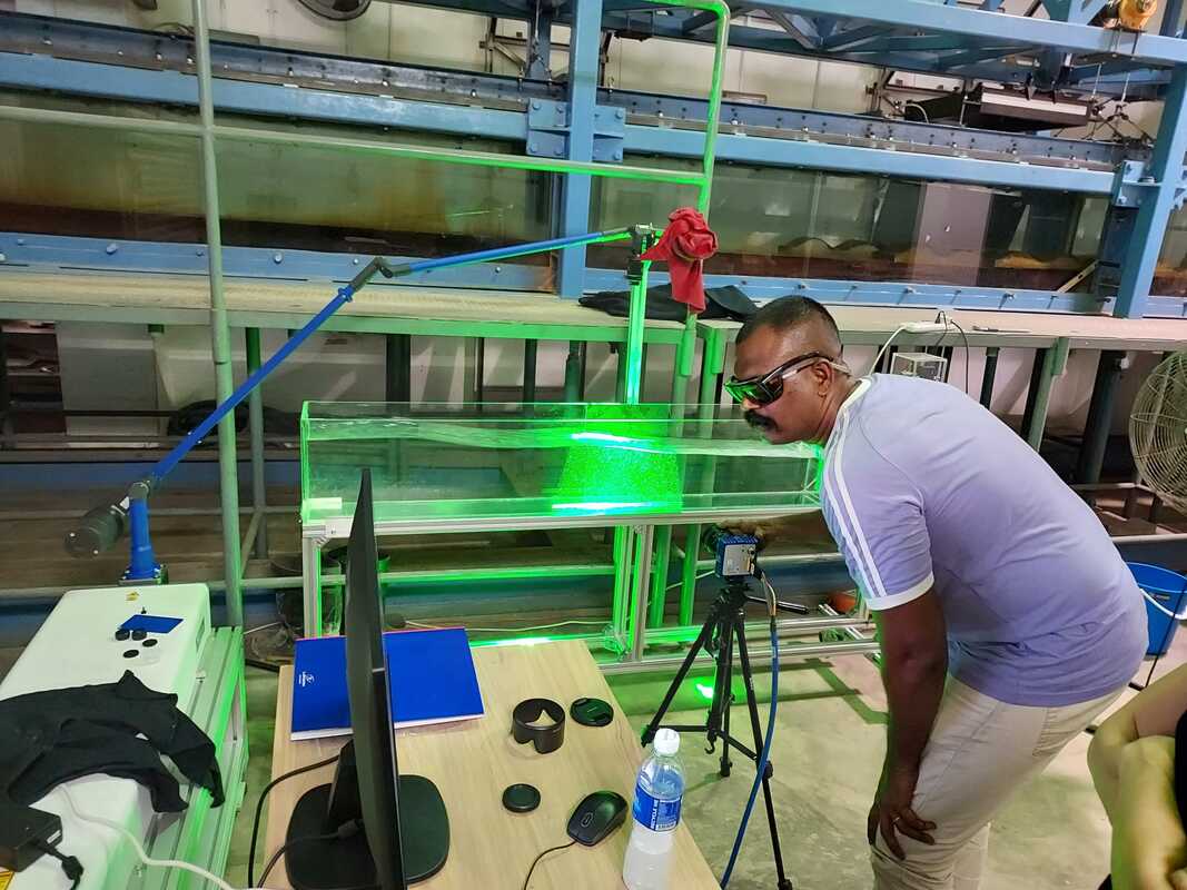
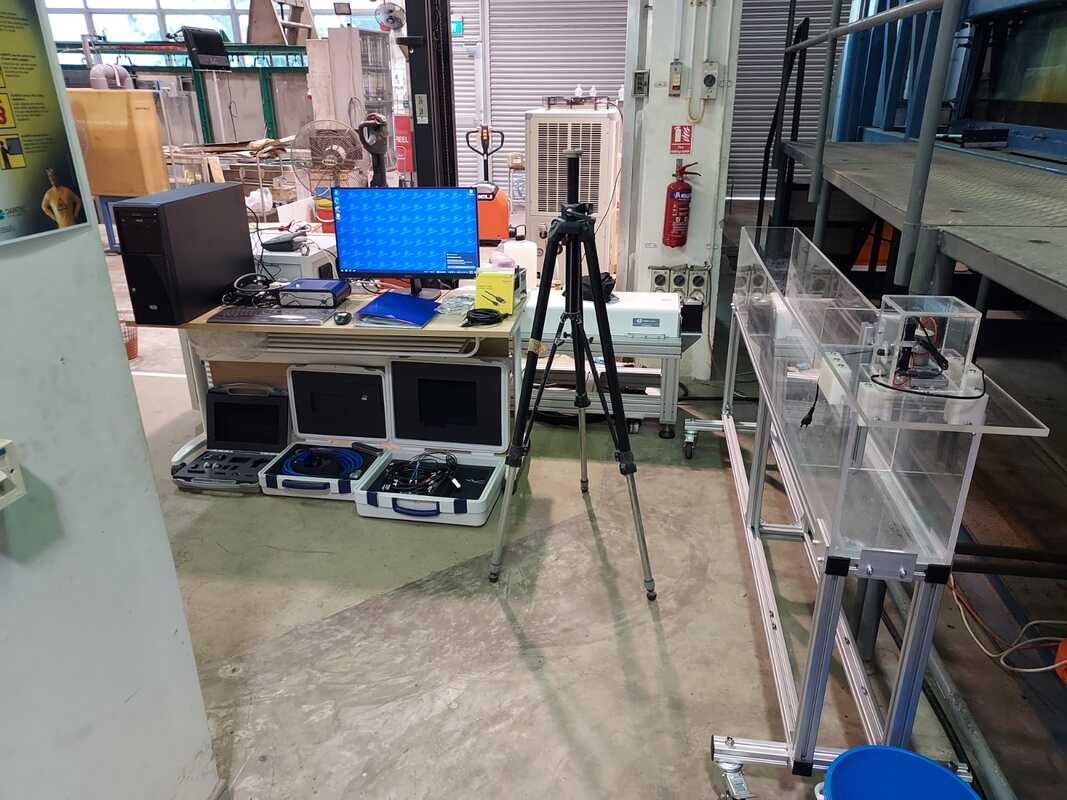
This LaVision High-Speed 2D PIV System is employed to acquire comprehensive insights into the swash flows generated by a train of solitary waves and the concurrent turbulence structure. This system conducts two-dimensional velocity measurements utilising a 100-Hz high-speed particle image velocimetry (HSPIV) technique.
0 Comments
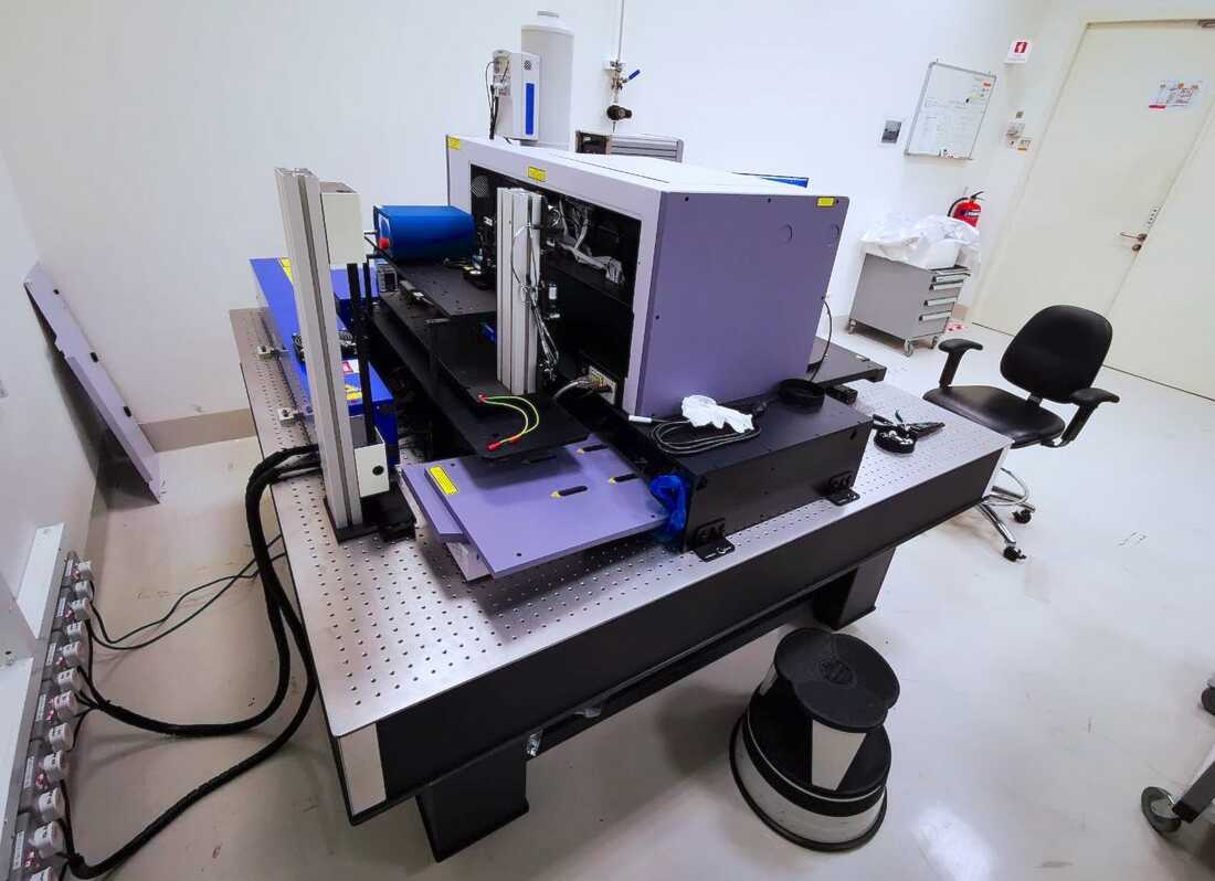
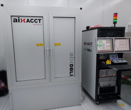 Our engineering team has assisted aixacct in the technical support in the aixDBLI system.
The Industrial Line DBLI systems offers manufacturers of piezoelectric MEMS products the ability to monitor quality in the production process for the first time. 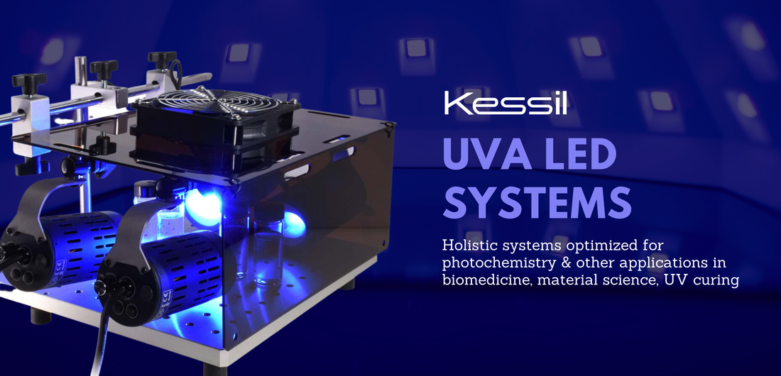 We are pleased to announce that Kessil products are now part of the offerings in Analytical Technologies. Kessil specializes in providing UVA LED solutions meticulously optimized for diverse applications, including photochemistry, biomedicine, material science, and UV curing.
Distinguished by its remarkable attributes, the Kessil UVA LED stands out with an impressive threefold increase in power compared to its competitors. This heightened irradiance capability translates to enhanced photoreactivity, while simultaneously ensuring a safer operational environment, extended operational lifespan, reduced heat emissions, and heightened environmental sustainability. Moreover, Kessil presents comprehensive holistic systems that are purposefully engineered for seamless integration. These systems serve to transform conventional setups into efficient photoreactors tailored for a spectrum of laboratory photocatalytic reactions. This versatility opens doors to applications ranging from direct photoexcitation to the activation of alkyl and aryl halides, while also encompassing photoreactor design aspects. The incorporation of Kessil products within these systems underscores their commitment to advancing innovation across multiple domains.
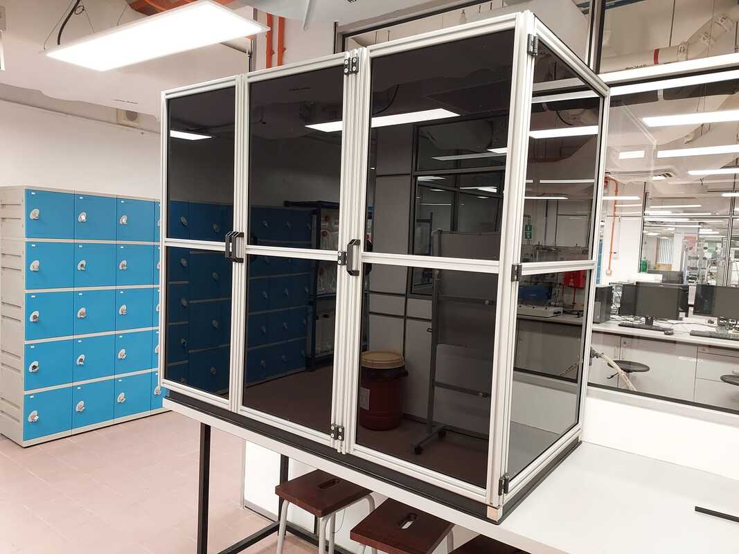
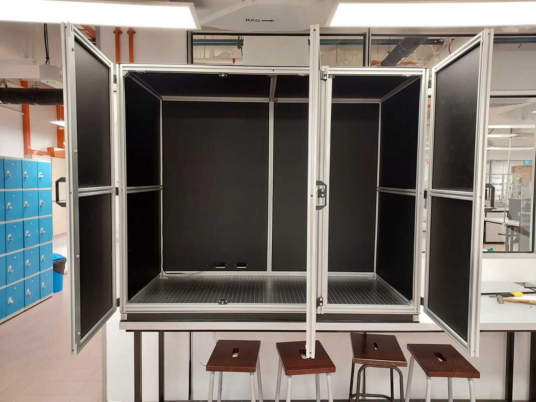
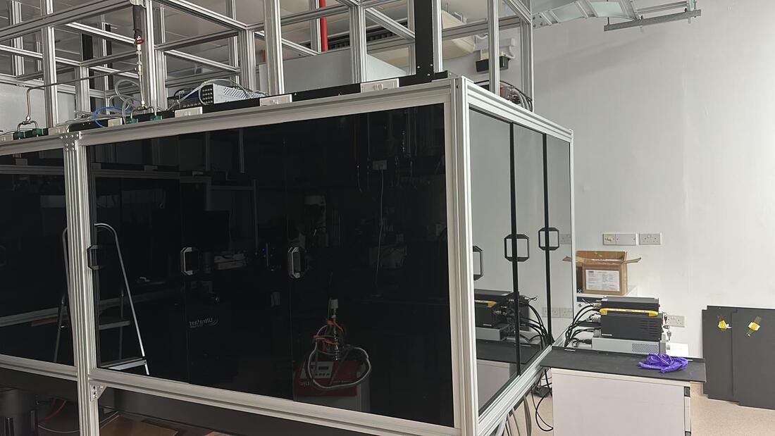
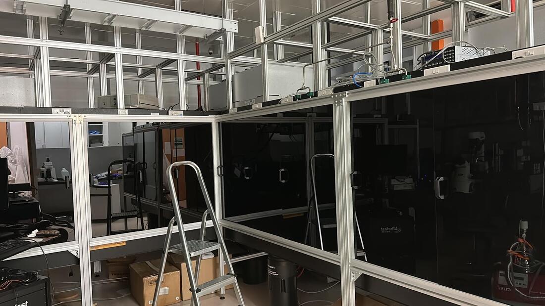
Looking for a controlled environment within an open lab for your experiments?
Our team of engineers specialises in crafting customised dark enclosures tailored to seamlessly fit your workspace. These enclosures not only provide the necessary controlled conditions but also come equipped with safety switches, ensuring a secure and optimised environment for your experiments.  This was a customised solutions that Analytical Technologies has worked with EVERBEING for probing onto your PCB boards, accommodating a range of sizes according to your specifications. Our stations seamlessly integrate with various applications, including DC, RF, mmW, and High Temperature capabilities. Certain models also support double-sided probing (top and bottom) for enhanced versatility.
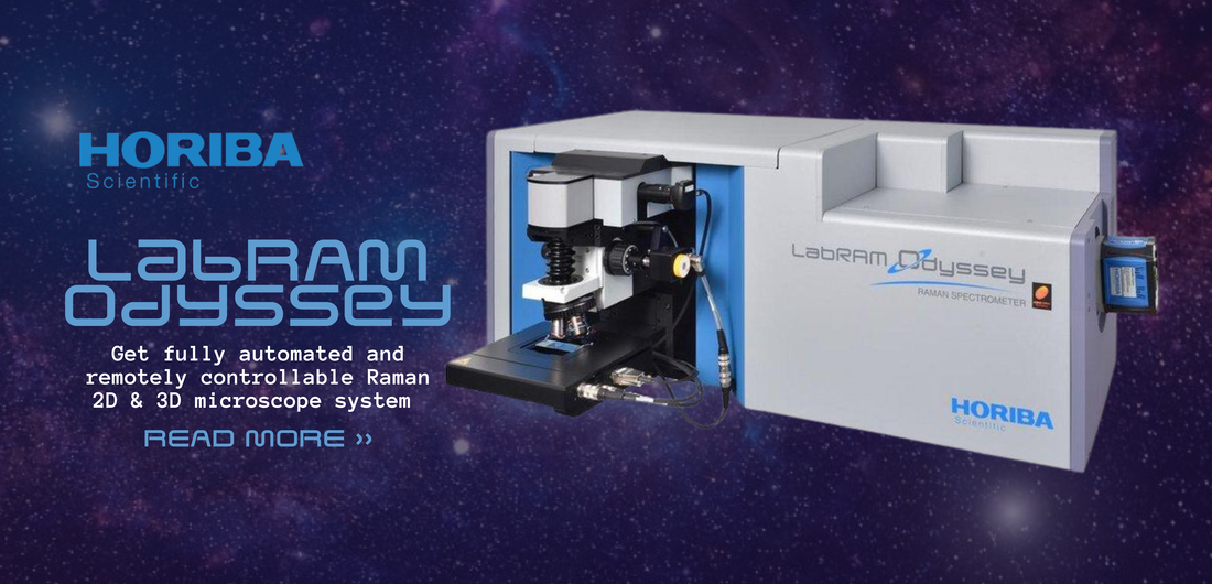 HORIBA Scientific, a global frontrunner in the realm of Raman microscopy, is pleased to unveil its latest innovation, the LabRAM Odyssey. This cutting-edge system represents a fully automated and remotely manageable solution.
The LabRAM Odyssey replaces the best seller LabRAM HR Evolution. Developed on the same platform, the LabRAM Odyssey is now more user friendly and offers new functionalities, advanced confocal imaging capabilities in 2D and 3D, and is fully compliant with all market requirements. The LabRAM Odyssey can also be configured to enable semiconductor process engineers to qualify the different steps in a timely manner, with a high level of confidence. The LabRAM Odyssey Semiconductor is the ideal tool for photoluminescence and Raman imaging on wafers up to 300 mm diameter with its 300 mm × 300 mm automated sample stage and its automated objective turret. It offers a high spatial resolution mode to detect and identify defects and submicron inhomogeneities to understand and give insight about their origin. 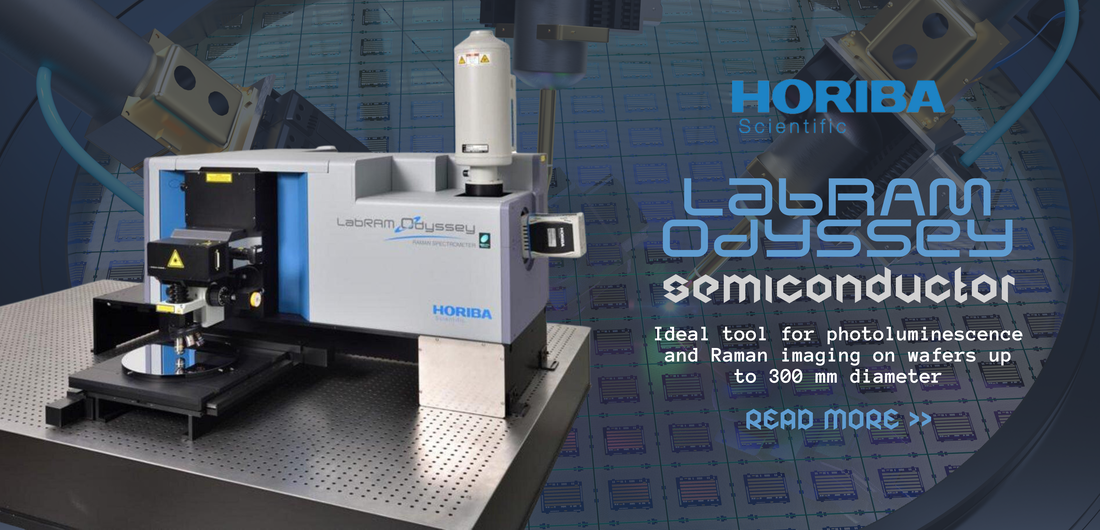 HORIBA is pleased to introduce the latest addition to its repertoire, the LabRAM Odyssey Semiconductor system. This pioneering Raman/Photoluminescence microscope derives its foundation from the widely acclaimed LabRAM HR Evolution Confocal Raman Microscope, renowned for its exceptional high resolution capabilities. Noteworthy enhancements include the integration of a sample mounting stage adept at accommodating the prevalent 300 mm wafer size, catering directly to the semiconductor industry's standard requirements.
A customised enclosure equipped with HEPA filters represents a crucial element for sensitive optical setups that require a controlled environment.
The enclosures are designed to provide an isolated and contaminant-free space to house sensitive and demanding optical instrumentation. For more customisation services, please contact us with your experiment requirements below.
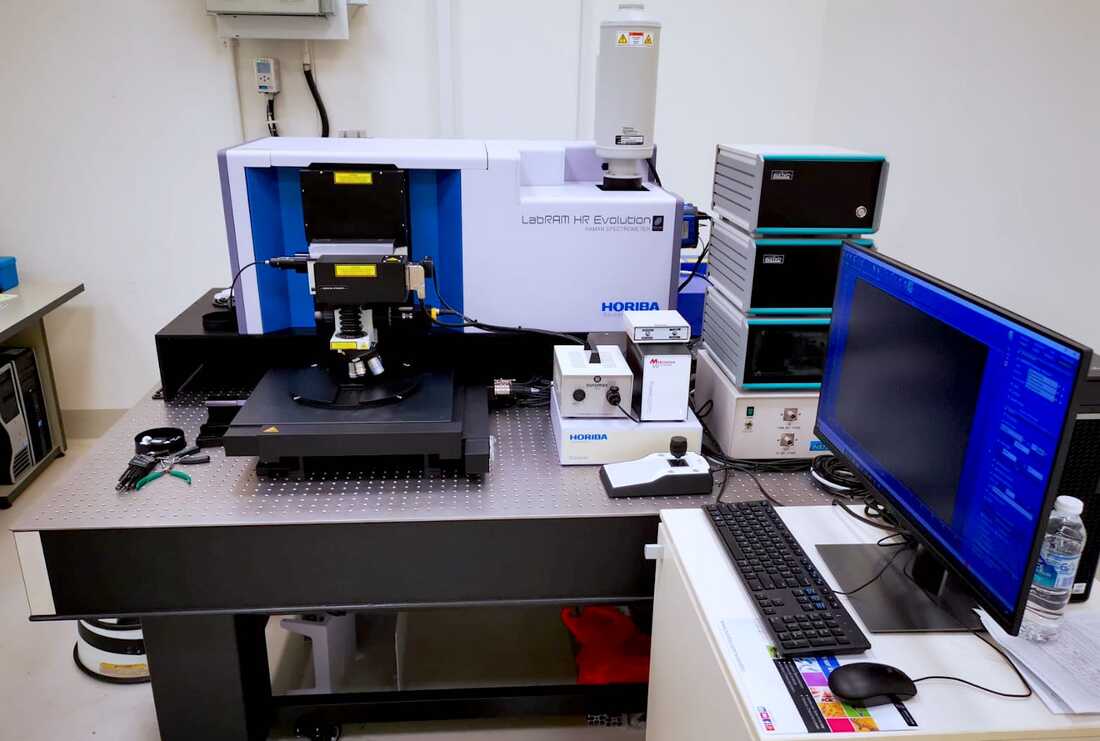
Our local technical support team has successfully commissioned a semiconductor variant of the world renowned LabRAM Evolution Confocal MicroRaman System. Fully equipped with multiple lasers from UV to NIR and unique upgrades, the system is able to handle Raman as well as Photoluminescence measurements.
The LabRAM Confocal MicroRaman system microscopes are ideally suited for both micro and macro measurements, and offer advanced confocal imaging capabilities in 2D and 3D. The true confocal Raman microscope enables the most detailed images and analyses to be obtained with speed and confidence. It is widely used for standard Raman analysis such as PhotoLuminescence (PL), it can also be further integrated for other hybrid analysis. NanoRaman set up with bipotentiostat for Tip Enhanced Raman Spectroscopy (TERS) application20/3/2023 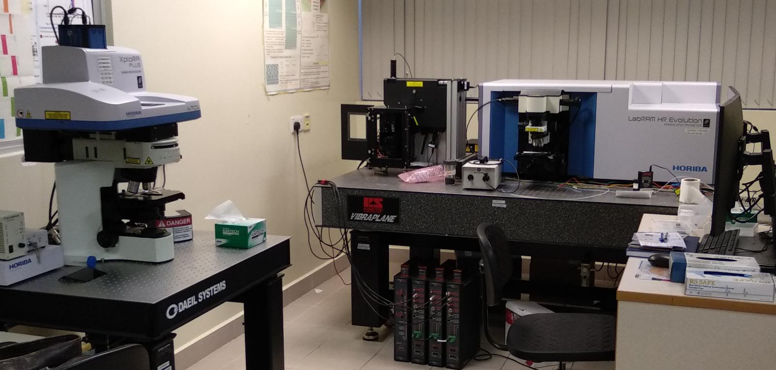 The NanoRaman system equipped with LabRAM Evolution being installed locally by Analytical Technologies' in-house team. LabRAM Evolution, the world renowned Raman solution for research and analysis. The integral flexibility of the LabRAM HR Evolution makes it the ideal platform for combined with the fully integral nano-Raman for research to TERS (tip enhanced Raman scattering). 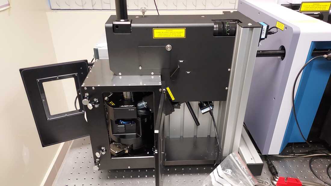 A close up of the integration of a customised environmental chamber and electrochemical cell within a NanoRaman (as shown above) setup designed a sophisticated and versatile experimental configuration to enhance the capabilities of this analytical instrument. This integrated system is further augmented by the inclusion of a bipotentiostat, a critical component for conducting Tip Enhanced Raman Spectroscopy (TERS) experiments. 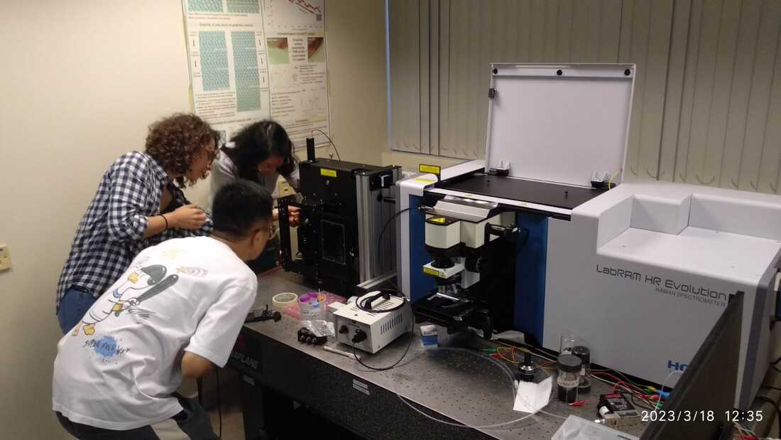 Personalised hands-on guidance and training provided by a HORIBA's application scientist represents a valuable and tailored educational experience designed to empower researchers, technicians, and users with the skills and knowledge required to make the most effective use of HORIBA's instruments. 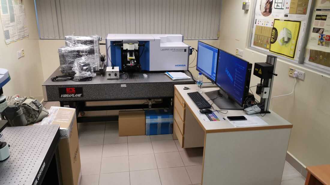 Another angle of the HORIBA's LabRAM HR Evolution Setup before the integration of NanoRaman, with HORIBA's in-house software installed in the computer (right).
|
HappeningsBesides keeping all informed about our current activities,we will also be showcasing some of our customers' works and research updates on this page.
Archives
October 2023
Categories
All
|
 RSS Feed